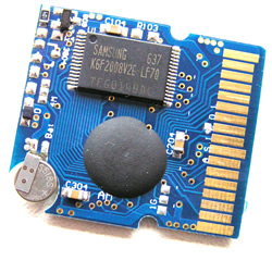
 Boot Card Technical Specification Boot Card Technical Specification
GENERAL DESCRIPTION AND FEATURES
• Voltage Supply : 2.7 V ~ 3.6 V
• Organization- Memory Cell Array : (1G + 32M)bit x 8bit- Data Register : (2K + 64)bit x8bit
• Automatic Program and Erase- Page Program : (2K + 64)Byte- Block Erase : (256K + 8K)Byte
• Page Read Operation- Page Size : (2K + 64)
• Byte- Random Read : 60µs(Max.)- Serial Access : 30ns(Min.)
• Memory Cell : 2bit / Memory Cell1G x 8 Bit / 2G x 8 Bit NAND Flash Memory
• Fast Write Cycle Time- Program time : 800µs(Type.)- Block Erase Time : 1.5ms(Type.)
• Command/Address/Data Multiplexed I/O Port
• Hardware Data Protection- Program/Erase Lockout During Power Transitions
• Reliable CMOS Floating-Gate Technology- Endurance :
• 5K Program/Erase Cycles(with 4bit/512byte ECC)- Data Retention : 10 Years
• Command Register Operation
• Unique ID for Copyright Protection
• Package : - K9G8G08U0M-PCB0/PIB0 : Pb-FREE PACKAGE48 - Pin
• TSOP I (12 x 20 / 0.5 mm pitch)- K9G8G08U0M-ICB0/IIB052 - Pin
• ULGA (12 x 17 / 1.00 mm pitch)- K9LAG08U1M-ICB0/IIB052 - Pin ULGA (12 x 17 / 1.00 mm pitch)
Download Data Sheet for DSKe Coin Cell Double Layer Capacitor [.PDF]
Flash Boot Card Functional Block Diagram

Product Introduction.
The K9G8G08U0M is a 8,448 Mbit (8,858,370,048 bit) memory organized as 524,288 rows (pages) by 2,112x8 columns. Spare 64 columns are located from column address of 2,048~2,111. A 2,112-byte data register is connected to memory cell arrays for accommodating data transfer between the I/O buffers and memory cells during page read and page program operations. The memory array is made up of 32 cells that are serially connected to form a NAND structure. Each of the 32 cells resides in a different page. A block consists of two NAND structured strings. A NAND structure consists of 32 cells. A cell has 2-bit data. Total 1,081,344 NAND cells reside in a block. The program and read operations are executed on a page basis, while the erase operation is executed on a block basis. The memory array consists of 4,096 separately erasable 256K-byte blocks. It indicates that the bit by bit erase operation is prohibited on the K9G8G08U0M.
Main Product Specifications
|