   |


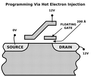
Device OperationPage read is initiated by writing 00h-30h to the command register along with five address cycles. After initial power up, 00h commandis latched. Therefore only five address cycles and 30h command initiates that operation after initial power up. The 2,112 bytes of datawithin the selected page are transferred to the data registers in less than 60µs(tR). The system controller can detect the completion ofthis data transfer(tR) by analyzing the output of R/B pin. Once the data in a page is loaded into the data registers, they may be readout in 30ns cycle time by sequentially pulsing RE. The repetitive high to low transitions of the RE clock make the device output thedata starting from the selected column address up to the last column address. The device may output random data in a page instead of the consecutive sequential data by writing random data output command.The column address of next data, which is going to be out, may be changed to the address which follows random data output com-mand. Random data output can be operated multiple times regardless of how many times it is done in a page. The device is programmed basically on a page basis, and the number of consecutive partial page programming operation within thesame page without an intervening erase operation must not exceed 1 time for the page. The addressing should be done in sequentialorder in a block. A page program cycle consists of a serial data loading period in which up to 2,112bytes of data may be loaded intothe data register, followed by a non-volatile programming period where the loaded data is programmed into the appropriate cell. The serial data loading period begins by inputting the Serial Data Input command(80h), followed by the five cycle address inputs andthen serial data loading. The words other than those to be programmed do not need to be loaded. The device supports random datainput in a page. The column address for the next data, which will be entered, may be changed to the address which follows randomdata input command(85h). Random data input may be operated multiple times regardless of how many times it is done in a page.The Page Program confirm command(10h) initiates the programming process. Writing 10h alone without previously entering theserial data will not initiate the programming process. The internal write state controller automatically executes the algorithms and tim-ings necessary for program and verify, thereby freeing the system controller for other tasks. Once the program process starts, theRead Status Register command may be entered to read the status register. The system controller can detect the completion of a pro-gram cycle by monitoring the R/B output, or the Status bit(I/O 6) of the Status Register. Only the Read Status command and Resetcommand are valid while programming is in progress. When the Page Program is complete, the Write Status Bit(I/O 0) may bechecked(Figure 8). The internal write verify detects only errors for "1"s that are not successfully programmed to "0"s. The commandregister remains in Read Status command mode until another valid command is written to the command register. The Erase operation is done on a block basis. Block address loading is accomplished in three cycles initiated by an Erase Setupcommand(60h). Only address A19to A30 is valid while A12to A18is ignored. The Erase Confirm command(D0h) following the blockaddress loading initiates the internal erasing process. This two-step sequence of setup followed by execution command ensures thatmemory contents are not accidentally erased due to external noise conditions.At the rising edge of WE after the erase confirm command input, the internal write controller handles erase and erase-verify. Whenthe erase operation is completed, the Write Status Bit (I/O 0) may be checked. Figure 10 details the sequence.
|
Copyright © 2006 Boot Card Inc. All rights reserved.
 PAGE READ